In recent years, affected by factors such as global semiconductor capacity shortages, the new crown epidemic, and seasonal demand, the prices of memory devices have shown relatively large fluctuations.
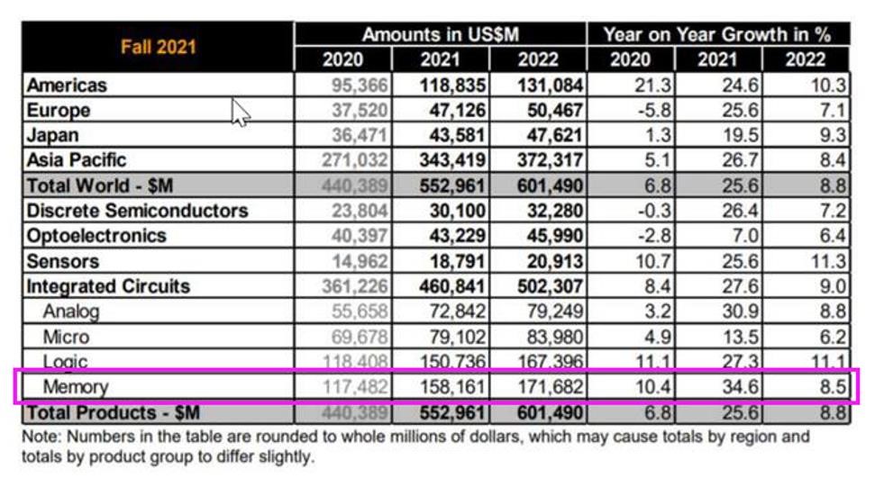
Analysts at major industry analysts including J.P. Morgan, Gartner and Deloitte have all predicted the shortage of semiconductor capacity to continue throughout 2022 and beyond. According to data analysis by WSTS, the size of the global memory device market in 2022 will reach US$171.682 billion, an increase of US$13.521 billion compared with the previous estimate in 2022, and a year-on-year growth of 8.5%.
As a memory device accounting for about 30% of the semiconductor chip industry, its demand is growing faster than the semiconductor industry. What is driving the market demand for memory devices? At present, mainstream applications such as 5G, Internet of Things, and cloud storage will continue to be the boosters of the traditional storage market; the explosion of the electric vehicle market has driven the demand for storage in the automotive electronics market; Size, power consumption and quality impose extremely demanding requirements; the rapid rise of artificial intelligence firmly binds sensing, storage and computing together. These emerging application scenarios will undoubtedly rely more on the technological development of embedded storage.
Compared with traditional storage devices, embedded storage has some unique advantages. Different application environments have their own requirements for embedded storage solutions. X-FAB, headquartered in Europe, the world’s leading analog and mixed-signal semiconductor fab, gave their own answer in this market—becoming a one-stop vehicle that provides a full range of embedded memory solutions Regulatory-level foundry: It includes different storage IPs such as OTP/MTP/EEPROM/EFLASH, and all embedded storage IPs have passed the highest specification automotive level, and the operating temperature can reach -40°C to +175°C between.
At present, the global semiconductor production capacity is in a state of extreme shortage. For those design companies that use stand-alone memory devices and integrate them through back-end SiP, they have to face potential production capacity risks from multiple suppliers. From the perspective of better allocation of chip production capacity, using SoC system design and adding embedded storage IP will undoubtedly achieve more efficient production capacity utilization. The advance layout of embedded solutions and production capacity will greatly increase the confidence that new products will be put into market mass production at the first time, so as to seize market opportunities. At the same time, compared with the SiP solution, the embedded solution saves more space, which means that the total cost of the overall design can also be optimized accordingly.
It can solve the urgent need of the memory chip market in short supply, and can obtain better time and price costs, and at the same time, it can also comply with the trend of miniaturization of system solutions. What exactly is such an embedded storage that kills three birds with one stone?
Take embedded non-volatile memory as an example, also known as eNVM, which is a type of memory chip. In contrast to stand-alone memory, embedded non-volatile memory chips are embedded inside the chip as part of its function. According to different principles and structures, embedded memory can be divided into one-time programmable (OTP) memory, multiple-time programmable (MTP) memory, flash memory (Flash) and electrically erasable programmable read-only memory (EEPROM). Due to different characteristics, the applicable fields are also different.
As we mentioned earlier, 5G, AI, cloud, automotive electronics and the Internet of Things are driving the growth of the memory market. So what is the “troika” that drives the growth of embedded memory? Now let’s talk about the real market demand and technological change of embedded storage.
If you want to ask what is the information processing mechanism in this world? Then the most simplified process is nothing more than perception, storage, computing and communication. When it comes to the hottest words in recent years, it must be sensing and artificial intelligence (Edge-AI). Let’s discuss embedding from these two perspectives. The advantages and development trend of the sensor.
The first is sensors. Today, more and more applications are relying on smart sensing devices, and smart sensors are increasingly demanding intelligence. This trend is often referred to as “smart sensor migration.” When the sensor is no longer a simple sensing, the requirement for the SoC chip is no longer simply to perform operations such as sensing or driving, but the ability to directly process the data captured from the outside world for the first time— – By supporting on-site adaptive processing, it is possible to quickly transform and optimize the data ready for transmission (making the data suitable for dissemination on the bus network or RF broadcast), so that the data can be further processed in the back end.
From the perspective of chip architecture, any smart sensor currently requires an on-board MCU for data computing and processing, and MCU is inseparable from SRAM and NVM (mainly EEPROM and Flash). The most basic function of the SoC is to convert the signals (mainly analog signals) captured by the sensor from the outside world into digital signals, and then convert the data according to different protocols at the back end for subsequent transmission. The key point that must be considered about the storage side in the entire system is the performance parameters of the storage unit, which in most cases depends on the application scenario of the entire SoC. Therefore, the storage solution used must have the ability to withstand the same working conditions of the entire system while ensuring that it can be perfectly integrated with the rest of the application in the system, and must also have the same level of reliability as the sensor or MCU itself. .
From this point of view, the advantages of embedded storage solutions will be very obvious. A typical example – the automotive and aerospace fields: In these fields, sensors must adapt to extreme high and low temperatures, while being able to withstand high voltages and sometimes even have the ability to recover from radiation. Similar to other applications, although the environmental requirements may not be as harsh, they still require relatively high safety standards, such as biomedical.
For the applications mentioned above, none of the existing alternatives to embedded solutions are cost-effective, less manageable, or even unable to match the sensor/MCU operating environment conditions. As a result, embedded solutions in these markets are expected to grow steadily in the future, led by global trends such as vehicle electrification, autonomous driving, and telemedicine.
Of course, when it comes to sensors, we have to mention low power consumption. Portable sensors are becoming more and more common in our daily life. In addition to still requiring these sensors to be smart enough in daily life, users also require “the ability to transform the sensed data into a useful user experience, or to compress the data for via wired or wireless networks (such as Bluetooth, cellular, etc.)”. In this process, users will pay more attention to the power consumption of the entire system, which refers to power drive or energy recovery. And embedded memory has its own advantages at this point.
Embedded solutions can ensure a SoC smoothly integrates low-power solutions (such as gate power supply), shortens the interconnection path, and minimizes possible antenna problems. Embedded solutions will also be less affected (or not affected at all) by parasitic leakage or other defects. For these defects, designers need to do extra work when choosing a heterogeneous approach to multiple packaged components.
In addition, in the miniaturization trend, many portable devices will face strict space constraints, such as medical wearable applications. Therefore, the size of electronic components has also become very critical. Embedded storage also has irreplaceable advantages in space saving. Similar applications, such as 3D integration, will greatly lead to the development of embedded memory, including resistive RAM or spintronic storage.
After talking about the intelligent and low-power trend of sensing, let’s talk about artificial intelligence (Edge-AI) that has the opportunity to reshape our future. In fact, in the long run, this trend is gradually transforming the current smart sensing into a new generation of smart sensing. More analysis and decision-making will be done by sensors that mimic human senses and reflexes. As mentioned earlier, in order to make new or existing applications more efficient, “intelligence” and “low power consumption” need to be perfectly combined. At present, especially in the face of power-driven solutions, the two major applications of image recognition and audio recognition will provide endless impetus for this transformation. Of course, with the continuous development of artificial intelligence, we will definitely see more new applications than we can imagine.
In the application field of artificial intelligence (Edge-AI), different types of neural network architectures are mostly implemented in silicon – all these implementations are based on semiconductor arrays and implement these basic MACs based on inference and machine learning. operate. This semiconductor cell array is conceptually very similar to embedded memory arrays, which heralds a future technology trend: from current logic arrays (volatile or non-volatile) to multi-bit multi-bit cells Or an upgrade to “near-simulation”.
The core point of the entire artificial intelligence (Edge-AI) is that this network connection structure similar to the storage architecture will no longer be a subsidiary of the CPU, but will become the computing center of the entire application. This differs from the traditional MCU-based approach, which uses a storage array to transfer data back and forth from the CPU (consuming a lot of power in the process, and generating additional heat). In the Edge-AI architecture, everything about computing is done inside the array, enabling true in-memory computing. Just as the human brain works, all decision-making occurs internally through electrical pathways between neurons and synaptic arrays.
Since artificial intelligence is widely considered to be another big event after the mobile phone revolution, it will grow at a double-digit compound growth rate in the next few years, and can greatly improve the way we live. Therefore, on this track, companies that have a full understanding of embedded memory and its integrated solutions will have the upper hand in the market. In the application of artificial intelligence, some key technical parameters depend more on:
• The operation framework of bit-cell
• Overall low power competitiveness
• Design flexibility for multiple NVM solutions
• The versatility of choosing the Foundry platform
Taken together, embedded storage is the perfect solution for many sensors that require intelligent support. And embedded memory, especially non-volatile memory, will usher in a very bright application prospect in the medium and long term. In the short term, embedded memory solutions can help alleviate the recent global semiconductor shortage and become a key enabler of innovation in automotive and portable applications, especially healthcare. In the long run, embedded storage can pave the way for Edge-AI to achieve mass adoption and popularization. In a sense, embedded storage will help mankind enter the next era of civilization.
It is worth mentioning that in order to meet the growing demand for embedded storage, X-FAB can provide a very flexible one-stop solution. The overall solution has first-class reliability quality, diverse and flexible collocation options, and a continuous and stable NVM platform, which can meet the different needs of customers. And X-FAB’s professional capabilities and complete technology roadmap will help its customers stand out from their competitors.
About X-FAB:
X-FAB is a leading analog/mixed-signal and MEMS foundry group producing silicon wafers for automotive, industrial, consumer, medical and other applications. X-FAB uses modular CMOS and SOI processes ranging in size from 1.0µm to 130nm, as well as its characteristic SiC and microelectromechanical systems (MEMS) long-life processes, to provide global customers with the highest quality standards, superior manufacturing processes and innovative solution. X-FAB’s analog-digital integrated circuits (mixed-signal ICs), sensor MEMS are produced at six production sites in Germany, France, Malaysia and the United States, and employs approximately 4,000 people worldwide.