High-side SmartFETs are gaining popularity due to their ease of use and high level of protection. Like standard MOSFETs, SmartFETs are ideal for a variety of automotive applications. The difference is the control circuitry built into the high-side SmartFET device. Control circuitry continuously monitors output current and device temperature while providing passive protection against voltage transients and other unexpected application conditions. This combination of active and passive protection features ensures a stable and reliable application scheme, extending the life of the device itself and the application load it protects.
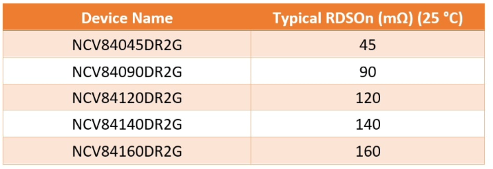
ON Semiconductor now offers a family of high-bridge SmartFETs from 45 mΩ to 160 mΩ. These devices are protected single-channel high-side drivers that switch a variety of loads such as light bulbs, solenoids, and other actuators. As shown in Table 1, the device names refer to the typical RDSon of the SmartFET at 25°C. The complete product range is listed below:
This series of devices from ON Semiconductor is packaged in SO8, which has a small footprint and provides high power at the same time. A family of pinouts from 45 mΩ to 140 mΩ devices provides convenience for designers, allowing one pinout for a variety of application loads. Depending on the current level required for a particular application, simply switch one device to the other. These devices drive 12 V automotive grounded loads and provide protection and diagnostic functions. This family of devices integrates advanced protection features such as active inrush current management, overtemperature shutdown with auto-restart, and active overvoltage clamping. A dedicated current sense pin provides accurate analog current monitoring of the output and fault indication for short-to-battery, short-to-ground, and open load detection for ON and OFF states. All diagnostic and current sense functions are disabled or enabled by an active high current detection disable pin (NCV84160 only) or an active high current detection enable pin (all other devices in this family).
The “ultimate requirement” for a high-side SmartFET is to switch the load, for which the market offers different alternatives. For example, relays have been used in the industry for a long time to switch various automotive loads, especially those that require high current to activate. As the weight and size of automotive parts and assemblies continues to decrease, there has been a transition from relays to semiconductor switches with smaller footprints, greater noise immunity and lower EMI.
High-side SmartFETs have become the mainstream SmartFET configuration in the automotive market, replacing the often simpler lower-side SmartFETs. Figure 1 shows an example of a high-side and low-side SmartFET configuration. The load of the upper-side SmartFET is always connected to ground by switching to the supply, while the load of the lower-side SmartFET is always connected to the supply by switching to ground. SmartFETs are usually installed in control units or ECUs. The load wire is the length of cable connecting the load to the pin connector on the ECU. Depending on the type of load and its location in the vehicle, this load line can be very long, increasing the likelihood of a chassis short to ground, which can severely stress the load in the lower-bridge SmartFET configuration.
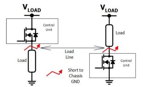
Figure 2 below shows the top-level block diagram and pinout of ON Semiconductor’s NCV84xxx high-bridge SmartFET family. Note that the high-side SmartFET is actually an NMOS FET with a regulated charge pump that pulls the gate voltage high enough to drive the load.
The input (IN) pin is a logic level pin used to turn the control logic/charge pump on and off for FET operation. The current sense enable (CS_EN) pin enables and disables the current sense function. The current sense (CS) pin feeds a proportional load current sense to the microcontroller for real-time feedback. This pin is multiplexed; it reports an analog fault event that is easily distinguishable from normal operation, allowing the user to detect output current or fault conditions in real time. The voltage (VD) pin is connected directly to the battery or power supply, and the OUT pin is connected to the load. Finally, the ground (GND) pin is just the GND of the device.
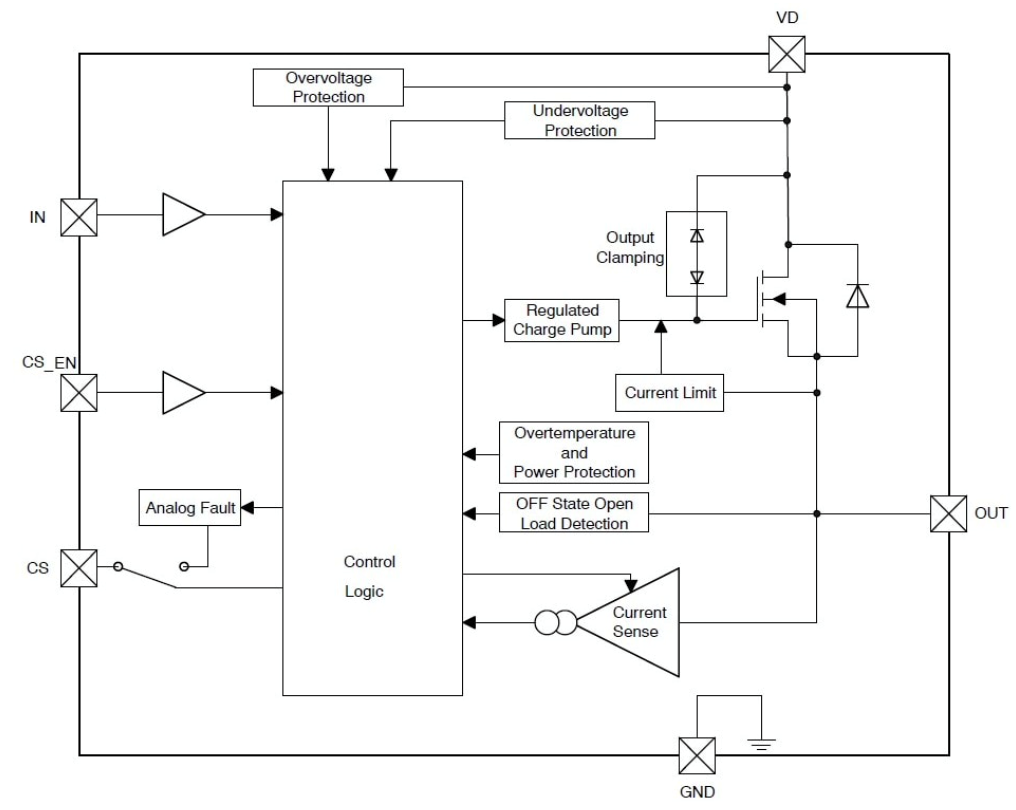
The NCV84xxx SmartFET family of devices offer the following protection features:
• Overvoltage protection protects the entire device, clamping VD-GND at voltages >41V.
• Brown-out protection, in a low battery condition, shuts down the device and waits for the battery voltage to rise high enough for the regulated charge pump to operate the FETs properly.
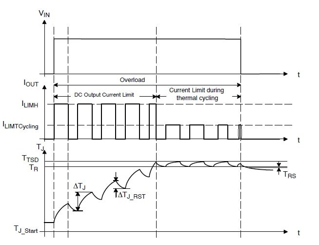
• Current limiting (see Figure 3 below) limits current to prevent damage in the event of a short circuit or surge event. Current will be limited until the device’s internal die temperature exceeds the overtemperature point, and will shut itself off for protection until it cools sufficiently. This feature is ideal for driving light bulb loads that require high initial inrush current, and also limits the amount of stress that high power and temperature fluctuations can place on the chip.
• Over-temperature and power-supply protection with auto-restart prevents the device from overheating due to high power consumption and excessive ambient temperature rise. If overtemperature protection is activated, the device will shut itself down until it cools sufficiently and automatically retry, assuming the input is “high”.
• Shutdown state open load detection alerts the microcontroller before entering “high” that the connection to the load has been lost in the shutdown state.
• Output clamp for inductive load switches, which safely turns on the FET to handle the inductor discharge current during inductor discharge.